IT之家 4月9日消息,根据首尔经济日报报道,三星电子开始研发1.0nm晶圆代工工艺,以图在与台积电的竞争中实现“技术翻盘”。
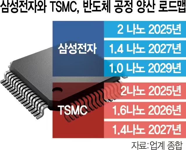
▲ 三星、台积电预测路线图,图源首尔经济日报
根据该日报报道,三星电子半导体研究所近日正式着手研发1.0nm工艺,部分曾参与2nm等尖端制程的研发人员被抽调,组建了专项项目团队。在目前三星公开的晶圆代工工艺路线图中,计划于2027年量产的1.4nm工艺为目前最尖端的工艺。

根据该日报所述,1nm工艺需要打破现有设计框架,引入新技术概念,以及引入高数值孔径极紫外(High-NA EUV)曝光设备等下一代设备。三星预计,量产时间将在2029年之后。

目前,三星在量产中的3nm工艺,以及预计在今年量产的2nm工艺,首尔经济日报认为技术上仍落后于台积电,尤其是2nm工艺方面,台积电的良率已突破60%,存在显著差距。因此,三星对1nm工艺寄予厚望,三星会长李在镕上月向高管们强调要“延续重视技术的传统”,并表示“以前所未有的技术引领未来”。

根据IT之家此前援引韩媒The Bell报道,三星目前最新的2nm SF2工艺初始良率“高于预期”,搭载该工艺的Exynos 2600芯片试产良率为30%。
Disclaimer: Investing carries risk. This is not financial advice. The above content should not be regarded as an offer, recommendation, or solicitation on acquiring or disposing of any financial products, any associated discussions, comments, or posts by author or other users should not be considered as such either. It is solely for general information purpose only, which does not consider your own investment objectives, financial situations or needs. TTM assumes no responsibility or warranty for the accuracy and completeness of the information, investors should do their own research and may seek professional advice before investing.